1 / 5
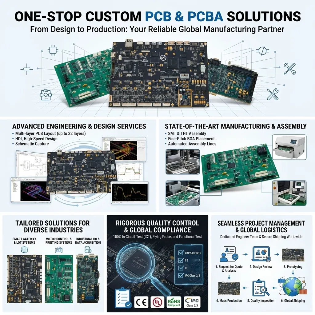
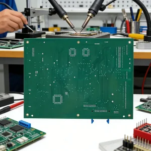
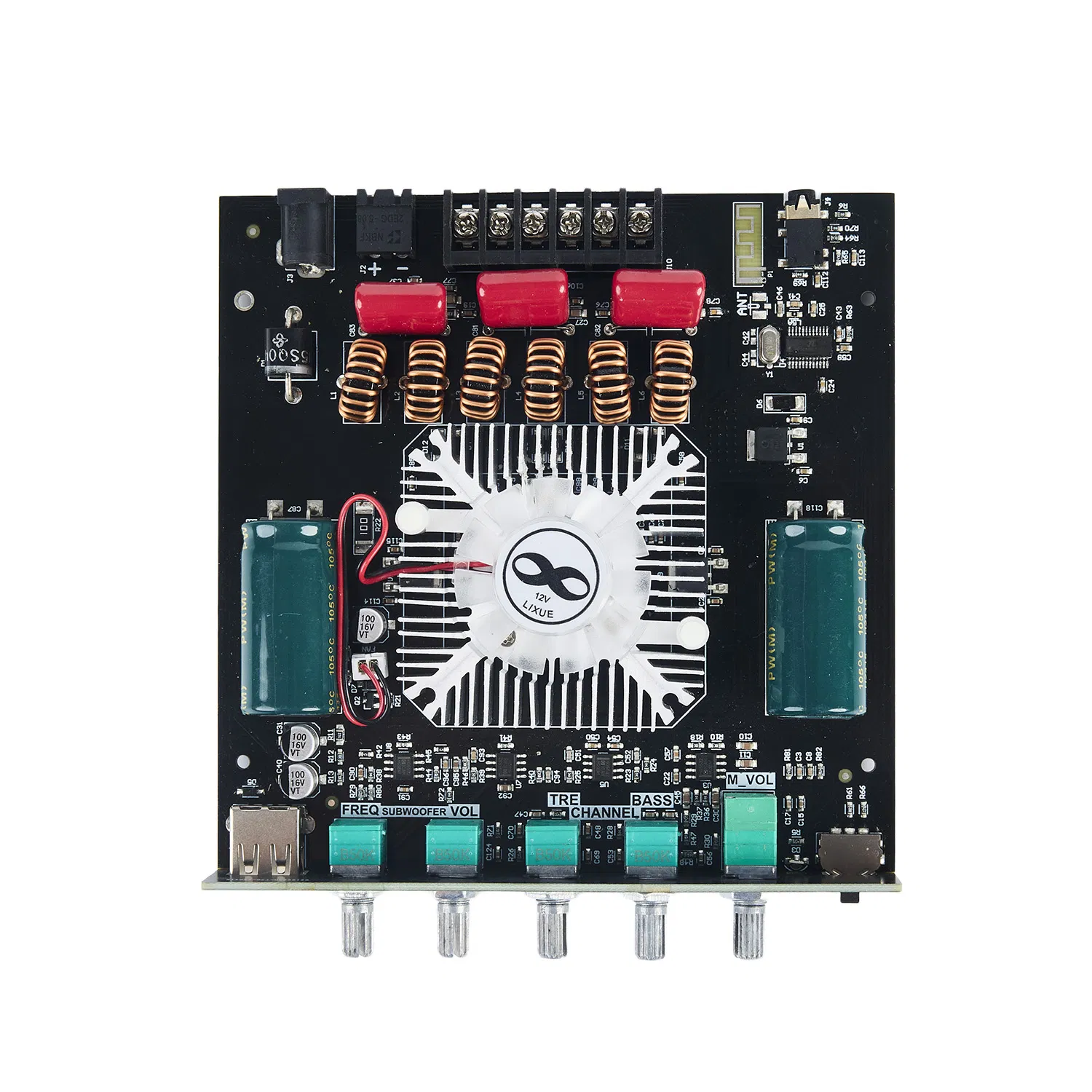
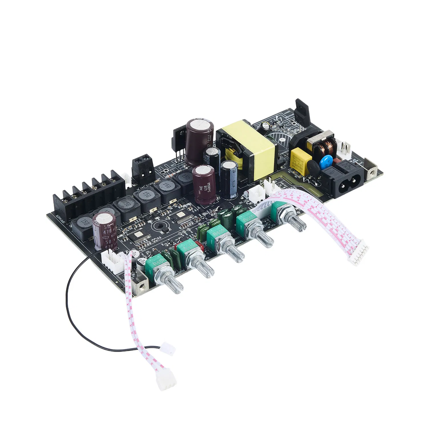
Transform your electronic designs with comprehensive PCB reverse engineering and PCBA manufacturing solutions that deliver exceptional quality and reliability. Our professional one-stop service covers everything from advanced circuit board analysis and precise cloning to full-scale production assembly and quality testing.
| Parameter | Detail |
|---|---|
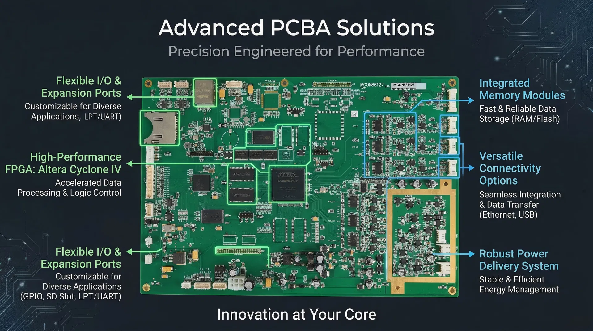
| Product Name | OEM PCBA Design |
| Copper Thickness | Customized |
| Applications | Communications, Automotive, Consumer Electronics |
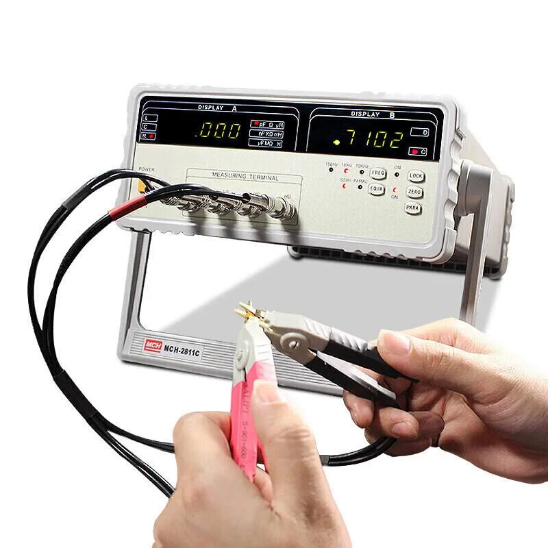
| PCB Testing | Flying Probe PCB Testing |
| Surface Treatments | HASL, LF-HASL, ENIG, IMM TIN, IMM AG, OSP |
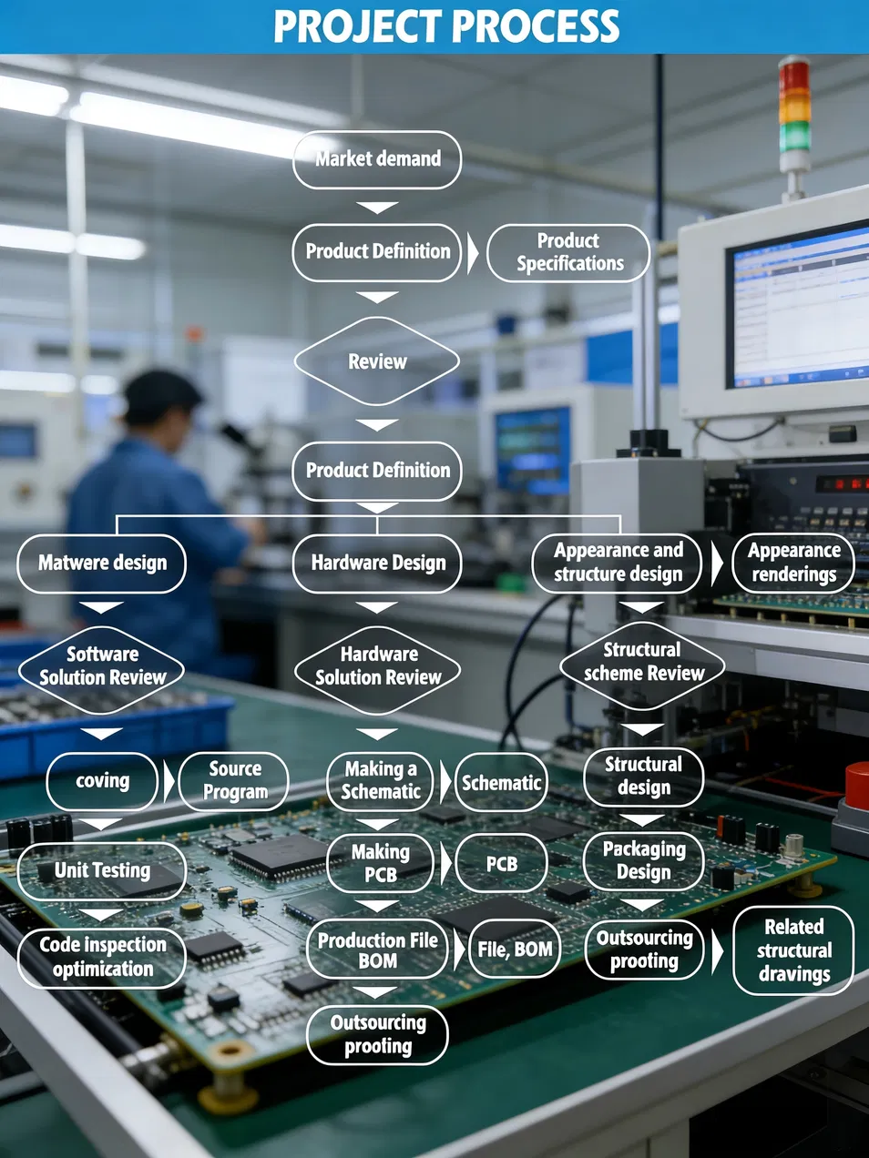
Our standardized end-to-end R&D process ensures precise project alignment and minimized trial-and-error costs. Includes Demand Validation, Firmware/Hardware/Mechanical design synchronization, and Prototyping Verification.
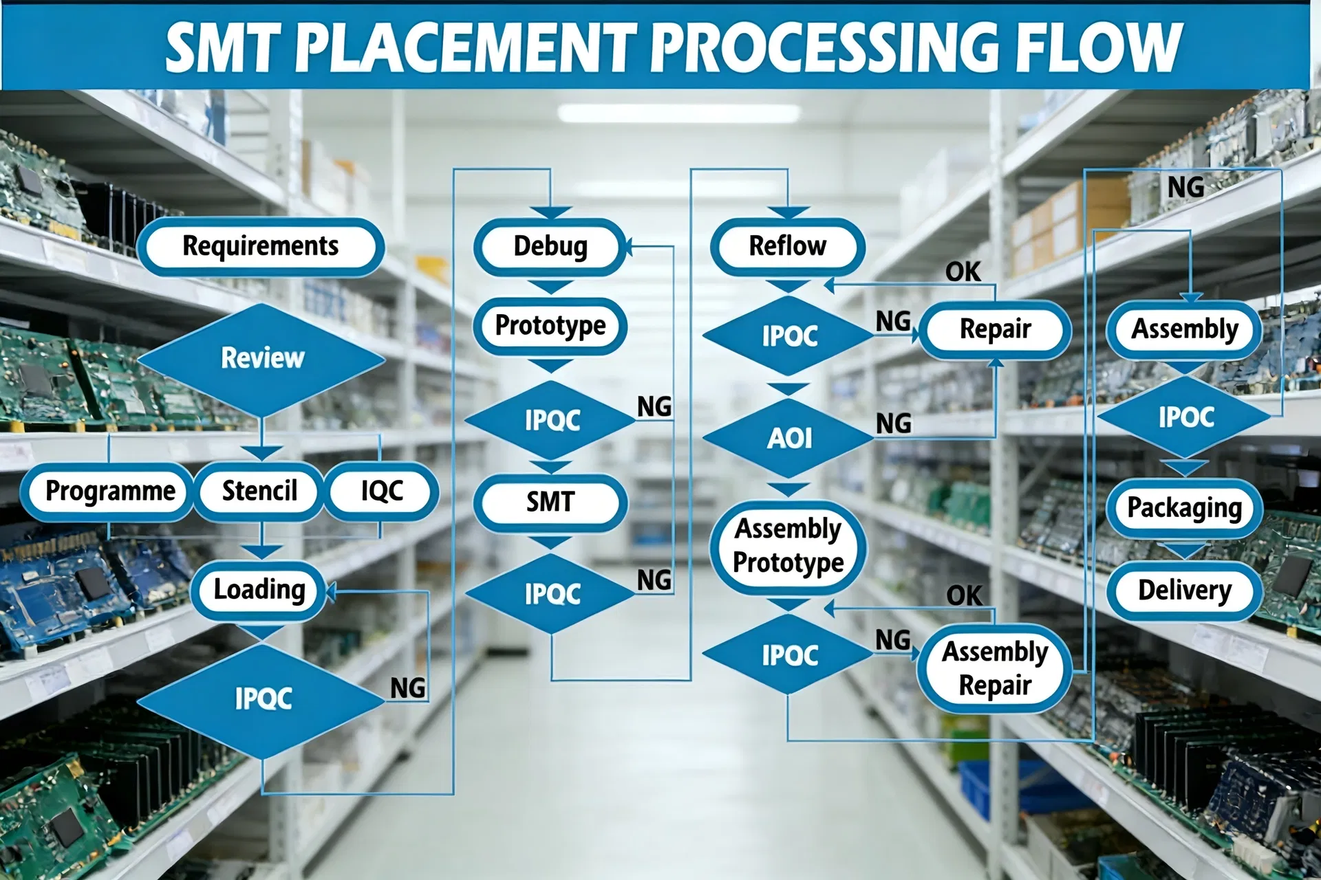
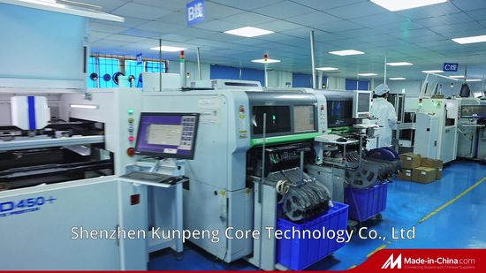
Closed-loop SMT production featuring full-process quality control, AOI (Automatic Optical Inspection), and stable batch consistency for ultra-high yield.
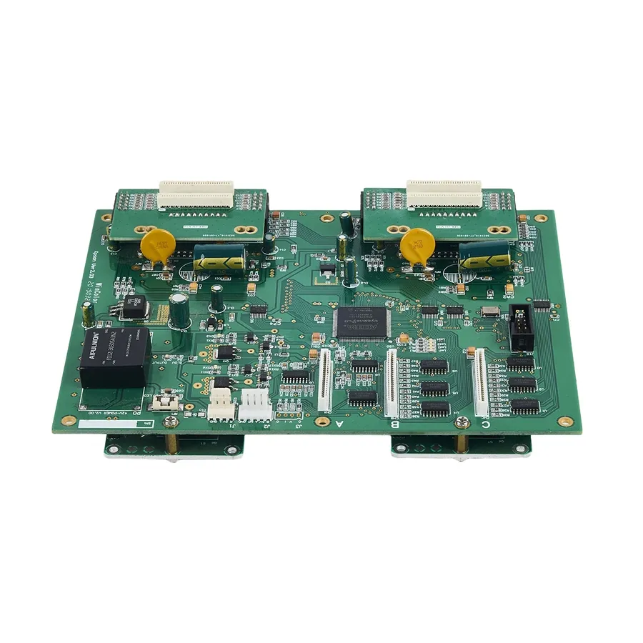
Bypass Legacy System Limitations: Reconstruct complete circuit designs from physical samples when original manufacturers discontinue support.
Scale Production Seamlessly: Transform from small-batch prototypes to high-volume production under one roof.
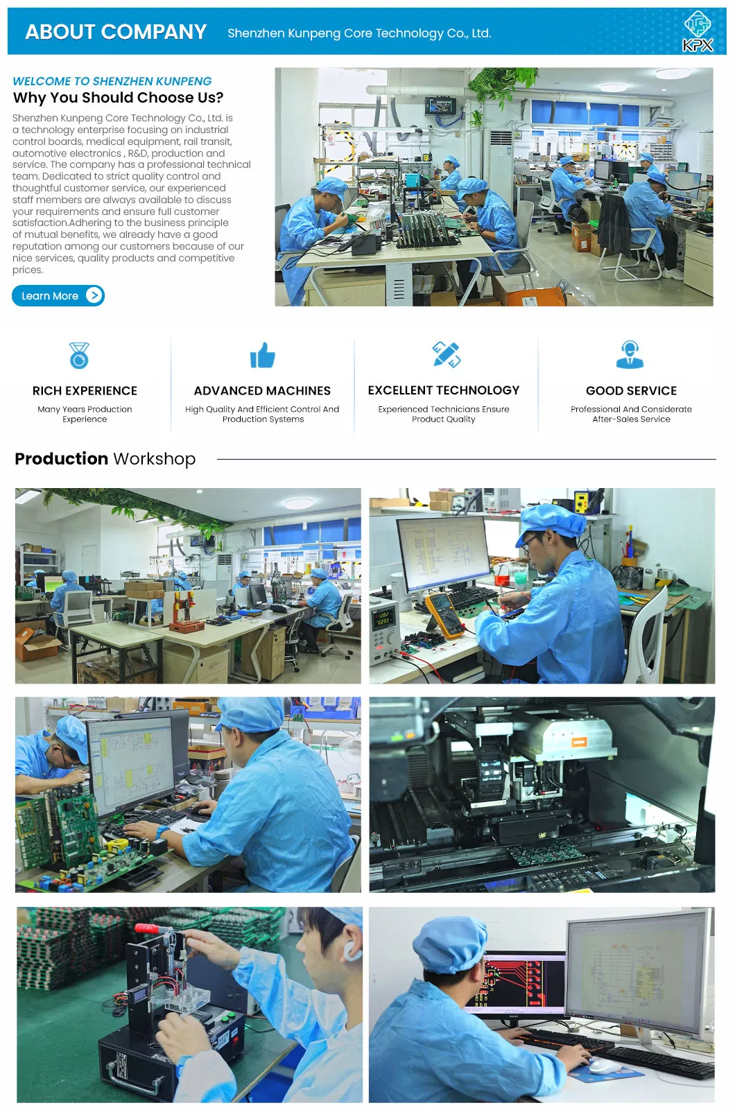
Specialized in industrial control, medical equipment, rail transit and automotive electronics, we provide one-stop R&D, production and technical services for PCBA/electronic assemblies. Backed by a seasoned technical team and advanced production facilities, we deliver high-quality, cost-effective products to global customers.